Coursetron engineering guide
DFT Scan Insertion Explained — Beginner to Industry Practice
DFT Scan Insertion Explained — Beginner to Industry Practice

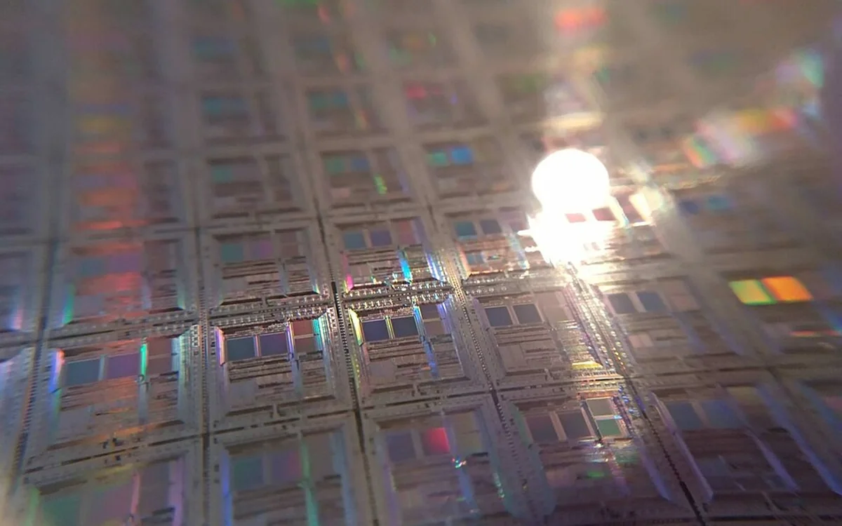
DFT Scan Insertion Explained
Design for Test (DFT) is what makes modern multi-billion-transistor SoCs testable in the fab. Without DFT, you cannot detect manufacturing defects and your yield collapses. This guide explains scan insertion from scratch.
What is Scan Insertion?
Scan converts regular flip-flops into scan flip-flops (mux-D scan cells). All scan flops in a chain form a shift register. ATE shifts in a known pattern, captures one cycle, shifts out the response, and compares with the expected golden pattern.
Scan Cell Types
- Mux-D scan: 1 extra mux on D input
- LSSD: Level-sensitive (mainstream IBM)
- Clocked scan
The DFT Flow
- Scan insertion: DC Topo / Tessent inserts mux-D cells
- Scan stitching: Chain ordering for routability
- ATPG: Tessent/TetraMAX generates test patterns
- BIST: Built-in self test for memories (MBIST) and logic (LBIST)
- JTAG/IEEE 1149.1: Boundary scan for board-level test
- Test compression: EDT/MaxTest cuts test time 10–100x
Coverage Metrics
- Stuck-at: aim for 99%+
- Transition delay: 90%+
- Path delay (timing-critical paths)
- Cell-aware (advanced node defects)
Career Outlook
DFT engineers are in critical short supply globally. Salaries: ₹6–10 LPA (fresher), ₹20–40 LPA (5+ years), $130K–$200K (US senior). See our DFT Course Online.
Leave a comment